NCP508
NCP508 is 50mA Low Dropout Voltage Regulator manufactured by onsemi.
Very Low Noise, Fast Turn On, 50 mA Low Dropout Voltage Regulator
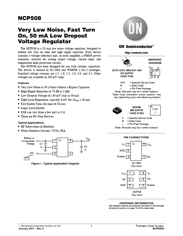
The NCP508 is a 50 mA low noise voltage regulator, designed to exhibit fast turn on time and high ripple rejection. Each device contains a voltage reference unit, an error amplifier, a PMOS power transistor, resistors for setting output voltage, current limit, and temperature limit protection circuits.
The NCP508 has been designed for use with ceramic capacitors. The device is housed in SC- 88A and WDFN6 1.5x1.5 packages. Standard voltage versions are 1.5, 1.8, 2.5, 2.8, 3.0, and 3.3. Other voltages are available in 100 mV steps.
Features
- Very Low Noise at 39 mVrms without a Bypass Capacitor
- High Ripple Rejection...