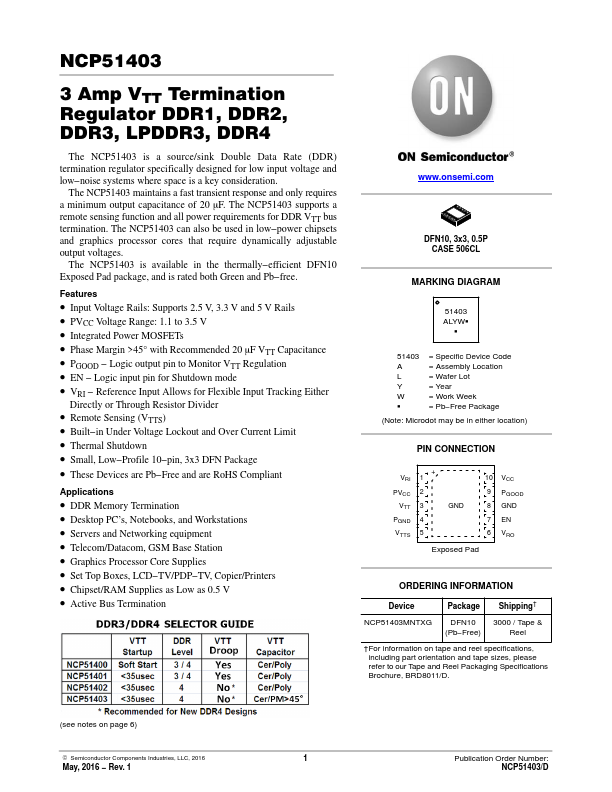
Datasheet4U Logo Datasheet4U.com

NCP51403 - Termination Regulator

Features

  • Input Voltage Rails: Supports 2.5 V, 3.3 V and 5 V Rails.
  • PVCC Voltage Range: 1.1 to 3.5 V.
  • Integrated Power MOSFETs.
  • Phase Margin >45° with Recommended 20 mF VTT Capacitance.
  • PGOOD.
  • Logic output pin to Monitor VTT Regulation.
  • EN.
  • Logic input pin.

📥 Download Datasheet

Datasheet Details

Part number NCP51403
Manufacturer onsemi
File Size 414.43 KB
Description Termination Regulator
Datasheet download datasheet NCP51403 Datasheet
Other Datasheets by ON Semiconductor

Full PDF Text Transcription

Click to expand full text
NCP51403 3 Amp VTT Termination Regulator DDR1, DDR2, DDR3, LPDDR3, DDR4 The NCP51403 is a source/sink Double Data Rate (DDR) termination regulator specifically designed for low input voltage and low−noise systems where space is a key consideration. The NCP51403 maintains a fast transient response and only requires a minimum output capacitance of 20 mF. The NCP51403 supports a remote sensing function and all power requirements for DDR VTT bus termination. The NCP51403 can also be used in low−power chipsets and graphics processor cores that require dynamically adjustable output voltages. The NCP51403 is available in the thermally−efficient DFN10 Exposed Pad package, and is rated both Green and Pb−free. Features • Input Voltage Rails: Supports 2.5 V, 3.
Published: |