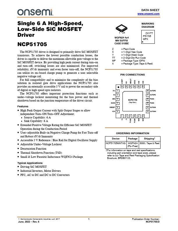
Datasheet4U Logo Datasheet4U.com

NCP51705 - Low-Side SiC MOSFET Driver

Datasheet Summary

Description

Pin # Name Description 1 IN+ Input for non

inverting, logic level PWM signal or ENABLE signal.

Input for inverting, logic level PWM signal or DISABLE signal.

Driver state flag.

See the application description for details.

Features

  • High Peak Output Current with Split Output Stages to allow independent Turn.
  • ON/Turn.
  • OFF Adjustment;.
  • Source Capability: 6 A.
  • Sink Capability: 6 A.
  • Extended Positive Voltage Rating for Efficient SiC MOSFET Operation during the Conduction Period.
  • User.
  • adjustable Built.
  • in Negative Charge Pump for Fast Turn.
  • off and Robust dV/dt Immunity.
  • Accessible 5 V Reference / Bias Rail for Digital Oscillator Supply.

📥 Download Datasheet

Datasheet preview – NCP51705

Datasheet Details

Part number NCP51705
Manufacturer ON Semiconductor
File Size 461.29 KB
Description Low-Side SiC MOSFET Driver
Datasheet download datasheet NCP51705 Datasheet
Additional preview pages of the NCP51705 datasheet.
Other Datasheets by ON Semiconductor

Full PDF Text Transcription

Click to expand full text
Single 6 A High-Speed, Low-Side SiC MOSFET Driver NCP51705 The NCP51705 driver is designed to primarily drive SiC MOSFET transistors. To achieve the lowest possible conduction losses, the driver is capable to deliver the maximum allowable gate voltage to the SiC MOSFET device. By providing high peak current during turn−on and turn−off, switching losses are also minimized. For improved reliability, dV/dt immunity and even faster turn−off, the NCP51705 can utilize its on−board charge pump to generate a user selectable negative voltage rail. For full compatibility and to minimize the complexity of the bias solution in isolated gate drive applications the NCP51705 also provides an externally accessible 5 V rail to power the secondary side of digital or high speed opto isolators.
Published: |