Datasheet Summary
3.0 A, Low Dropout Linear
Regulator with Enhanced ESD
Protection
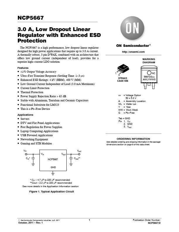
The NCP5667 is a high performance, low dropout linear regulator designed for high power applications that require up to 3.0 A current. A thermally robust, 3 pin D2PAK, bined with an architecture that offers low ground current (independent of load), provides for a superior high- current LDO solution.
Features
- ±1% Output Voltage Accuracy
- Ultra- Fast Transient Response (Settling Time: 1- 3 ms)
- Enhanced ESD Ratings: 4 kV (HBM), 400 V (MM)
- Low Ground Current Independent of Load (3.0 mA Maximum)
- Current Limit Protection
- Thermal Protection
- Power Supply Rejection Ratio > 65 dB
- Stable with Aluminum, Tantalum...