NCP57302
NCP57302 is Very Low-Dropout (VLDO) Fast Transient Response Regulator manufactured by onsemi.
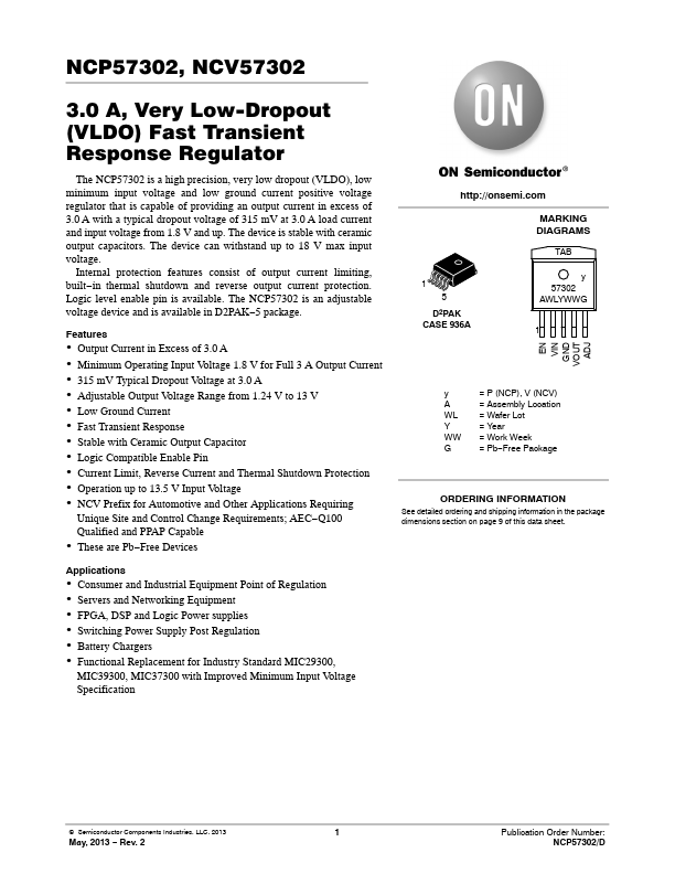
NCP57302, NCV57302
3.0 A, Very Low-Dropout
(VLDO) Fast Transient
Response Regulator
The NCP57302 is a high precision, very low dropout (VLDO), low minimum input voltage and low ground current positive voltage regulator that is capable of providing an output current in excess of 3.0 A with a typical dropout voltage of 315 mV at 3.0 A load current and input voltage from 1.8 V and up. The device is stable with ceramic output capacitors. The device can withstand up to 18 V max input voltage.
Internal protection Features consist of output current limiting, built- in thermal shutdown and reverse output current protection. Logic level enable pin is available. The NCP57302 is an adjustable voltage...