NCP7815
Description
Ground; Device Substrate. Symbol Value Unit Input Voltage Range (for Vout: 5.0 - 15 V) Vin -0.3 to 35 V Power Dissipation PD Internally Limited W Maximum Junction Temperature TJ(max) 150 °C Storage Temperature Range Tstg -65 to +150 °C ESD Capability, Human Body Model (Note 2) NCP7805, NCP7808 ESDHBM 4 kV NCP7812, NCP7815 3 ESD Capability, Machine Model (Note 2) ESDMM 400 V Stresses exceeding ESD Human Body Model tested per EIA/JESD22-A114 ESD Machine Model tested per EIA/JESD22-A115 Latchup Current Maximum Rating: ≤150 mA per JEDEC standard: JESD78 Table 3.
Key Features
- Output Current in Excess of 1.0 A
- Internal Thermal Overload Protection
- Internal Short Circuit Current Limiting
- Output Transistor Safe-Area pensation
- Output Voltage Offered in 4% Tolerance
- Available in Standard 3-Lead Transistor Packages
- For Tighter Tolerances and Extended Operating Range Refer to MC7800
- Enhanced ESD Tolerance: HBM 4 kV (5 V and 8 V Options), 3 kV (12 V and 15 V Options), and MM 400 V
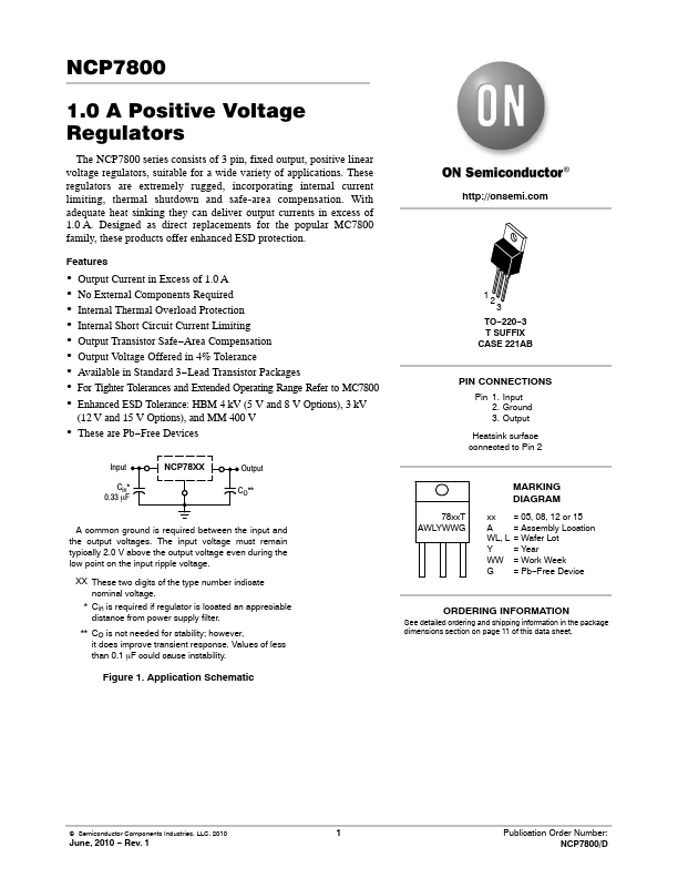
- Application Schematic http://onsemi. 12 3 TO-220-3 T SUFFIX CASE 221AB - Input