NCP81253
Features
- Space- efficient 2 mm x 2 mm DFN8 Thermally- enhanced Package
- VCC Range of 4.5 V to 5.5 V
- Internal Bootstrap Diode
- 5 V 3- stage PWM Input
- Diode Braking Capability via EN Mid- state
- Adaptive Anti- cross Conduction Circuit Protects against
Cross- conduction during FET Turn- on and Turn- off
- Output Disable Control Turns Off both MOSFETs via Enable Pin
- VCC Undervoltage Lockout
- These devices are Pb- free, Halogen- free/BFR- free and are Ro HS pliant
Typical Applications
- Power Solutions for Notebook and Desktop Systems
.onsemi.
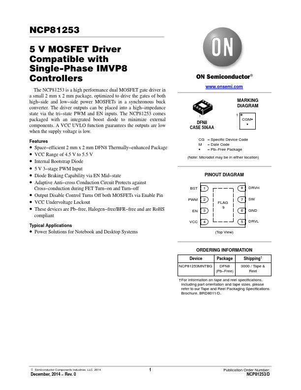
DFN8 CASE 506AA
MARKING DIAGRAM
1 CGMG G
CG = Specific Device Code M = Date Code G = Pb- Free Package
(Note: Microdot may be in either location)
PINOUT DIAGRAM
BST 1 PWM 2
EN 3 VCC 4
8 DRVH
FLAG 9
7 SW 6 GND
5 DRVL (Top View)
ORDERING INFORMATION
Device
Package
Shipping†
NCP81253MNTBG DFN8
3000 / Tape &
(Pb- Free)
Reel
†For information on tape and reel specifications, including part orientation and tape sizes, please refer to our...