NCS2540
Key Features
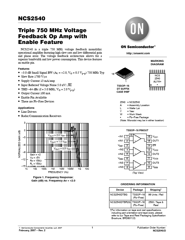
- 3.0 dB Small Signal BW (AV = +2.0, VO = 0.5 Vp-p) 750 MHz Typ
- Slew Rate 1700 V/ms
- Supply Current 13 mA/amp
- Input Referred Voltage Noise 5.0 nV/ǸHz
- THD -64 dBc (f = 5.0 MHz, VO = 2.0 Vp-p)
- Output Current 100 mA
- Enable Pin Available
- These are Pb-Free Devices
Applications
- Radar/munication Receivers