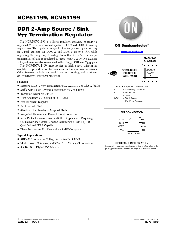
Datasheet4U Logo Datasheet4U.com

NCV51199 - Termination Regulator

General Description

Pin No.

Input voltage which supplies current to the output pin.

CIN = 470 mF with low ESR.

Key Features

  • include source/sink current limiting, soft.
  • start and on.
  • chip thermal shutdown protection. Features.
  • Supports DDR.
  • 2 VTT Termination to ±2 A, DDR.
  • 3 to ±1.5 A (peak).
  • Stable with 10 mF Ceramic Capacitance on VTT Output.
  • Integrated Power MOSFETs.
  • High Accuracy VTT Output at Full.
  • Load.
  • Fast Transient Response.
  • Built.
  • in Soft.
  • Start.
  • Shutdown for Standby or Suspend Mode.
  • Integr.

📥 Download Datasheet

Datasheet Details

Part number NCV51199
Manufacturer onsemi
File Size 74.59 KB
Description Termination Regulator
Datasheet download datasheet NCV51199 Datasheet

Full PDF Text Transcription (Reference)

The following content is an automatically extracted verbatim text from the original manufacturer datasheet and is provided for reference purposes only.

View original datasheet text
NCP51199, NCV51199 DDR 2-Amp Source / Sink VTT Termination Regulator The NCP/NCV51199 is a linear regulator designed to supply a regulated VTT termination voltage for DDR−2 and DDR−3 memory applications. The regulator is capable of actively sourcing and sinking ±2 A peak currents for DDR−2, and DDR−3 up to ±1.5 A while regulating the VTT output voltage to within ±10 mV. The output termination voltage is regulated to track VDDQ / 2 by two external voltage divider resistors connected to the PVCC, GND, and VREF pins. The NCP/NCV51199 incorporates a high−speed differential amplifier to provide ultra−fast response to line and load transients. Other features include source/sink current limiting, soft−start and on−chip thermal shutdown protection.