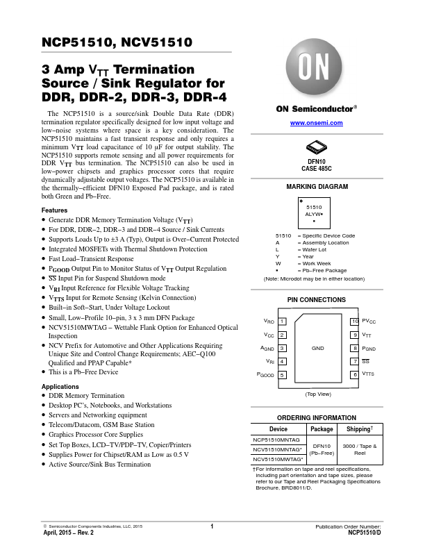
Datasheet4U Logo Datasheet4U.com
onsemi logo

NCV51510

Manufacturer: onsemi

NCV51510 datasheet by onsemi.

NCV51510 datasheet preview

NCV51510 Datasheet Details

Part number NCV51510
Datasheet NCV51510-ONSemiconductor.pdf
File Size 141.75 KB
Manufacturer onsemi
Description Termination Source / Sink Regulator
NCV51510 page 2 NCV51510 page 3

NCV51510 Overview

Pin Number Pin Name Pin Function 1 VRO OUTPUT − Buffered Output of VRI Reference Input pin. 2 VCC INPUT − Regulator Analog Power Input pin. Connect to the system supply voltage.

NCV51510 Key Features

  • Generate DDR Memory Termination Voltage (VTT)
  • For DDR, DDR-2, DDR-3 and DDR-4 Source / Sink Currents
  • Supports Loads Up to ±3 A (Typ), Output is Over-Current Protected
  • Integrated MOSFETs with Thermal Shutdown Protection
  • Fast Load-Transient Response
  • PGOOD Output Pin to Monitor Status of VTT Output Regulation
  • SS Input Pin for Suspend Shutdown mode
  • VRI Input Reference for Flexible Voltage Tracking
  • VTTS Input for Remote Sensing (Kelvin Connection)
  • Built-in Soft-Start, Under Voltage Lockout
onsemi logo - Manufacturer

More Datasheets from onsemi

View all onsemi datasheets

Part Number Description
NCV51511 High Side and Low Side Gate Driver
NCV51513 Automotive 130V High and Low Side Driver
NCV51561 Dual Channel Gate Driver
NCV5104 Half Bridge Driver
NCV5106A 600V Automotive High and Low Side Driver
NCV5106B 600V Automotive High and Low Side Driver
NCV511 Low-Dropout Voltage Regulator
NCV51152 Single Channel Gate Driver
NCV51190 1.5A DDR Memory Termination Regulator
NCV51198 1.5A DDR Memory Termination Regulator

NCV51510 Distributor

Datasheet4U Logo
Since 2006. D4U Semicon. About Datasheet4U Contact Us Privacy Policy Purchase of parts