NCV57201
Description
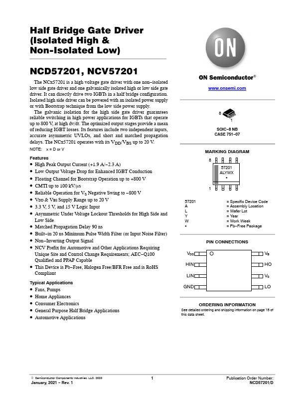
VDD HIN LIN GND 1 Power Low side and main power supply.
Key Features
- High Peak Output Current (+1.9 A/-2.3 A)
- Low Output Voltage Drop for Enhanced IGBT Conduction
- Floating Channel for Bootstrap Operation up to +800 V
- CMTI up to 100 kV/ms
- Reliable Operation for VS Negative Swing to -800 V
- VDD & VBS Supply Range up to 20 V
- 3.3 V, 5 V, and 15 V Logic Input
- Asymmetric Under Voltage Lockout Thresholds for High Side and Low Side
- Matched Propagation Delay 90 ns
- Built-in 20 ns Minimum Pulse Width Filter (or Input Noise Filter)
Applications
- Home Appliances