NCV7451
Features
- 5 V ±2% / 250 m A LDO
- Current Limitation with Fold- back
- Output Voltage Monitoring
- One High- Speed CAN FD Transceiver
- pliant to ISO11898- 2:2016
- CAN FD Timing Specified up to 5 Mbps
- Current Limitation, Reverse Current Protected
- Tx DC Timeout
- Local Wake- up parator
- Integrated Pull- up / Pull- down Current Source
- Very Low Current Quiescent Consumption
- Window Watchdog
- Direct Control
- Thermal Shutdown Protection
- AEC- Q100 Qualified and PPAP Capable
- Wettable Flank Package for Enhanced Optical Inspection
- This is a Pb- Free Device
Typical Applications
- Automotive
- Industrial Networks
.onsemi.
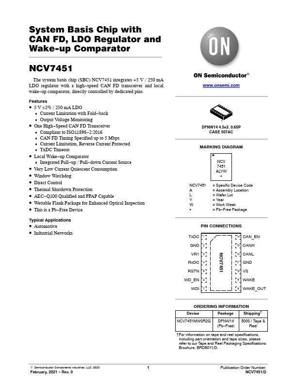
DFNW14 4.5x3, 0.65P CASE 507AC
MARKING DIAGRAM
NCV 7451 ALYW
NCV7451 A L Y W G
= Specific Device Code = Assembly Location = Wafer Lot = Year = Work Week = Pb- Free Package
PIN CONNECTIONS
Tx DC 1 GND 2 VR1 3 Rx DC 4 RSTN 5 WD_EN 6 WDI 7
14 CAN_EN 13 CANH 12 CANL 11 GND 10 VS 9 WAKE 8 WAKE_OUT
ORDERING INFORMATION
Device
Package
Shipping†
NCV7451MW...