Description
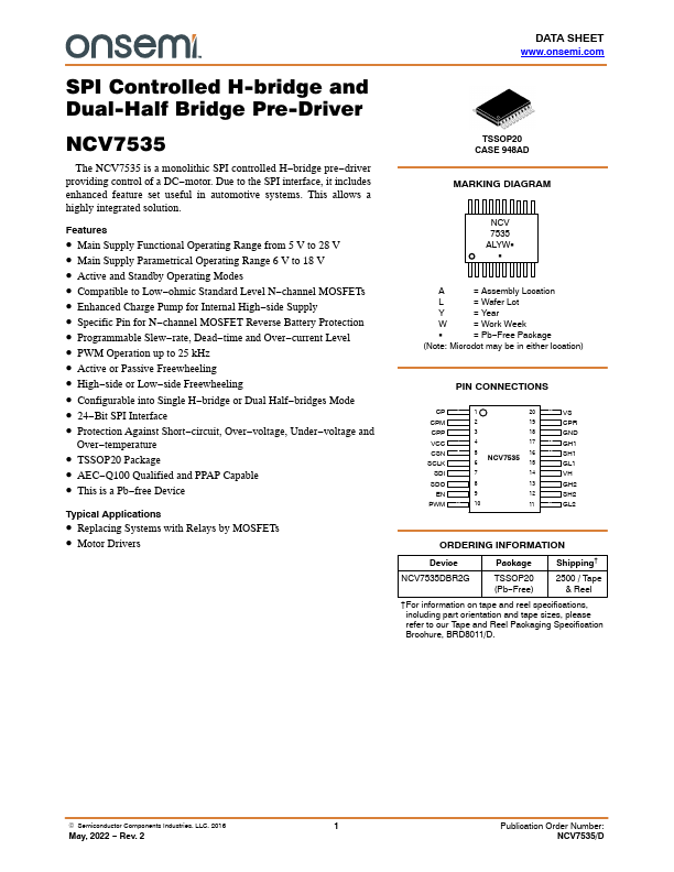
Charge pump output for high-side gate drive supply Minus terminal for pump capacitor Plus terminal for pump capacitor Logic supply of the device SPI chip select input SPI clock input SPI data input SPI data output Enable input Input for pulse width modulated driver duty cycle Output to gate of low-side switch 2 Connection to source of high-side switch 2 Output to gate of high-side switch 2 Connection to drain of high-side switched for short circuit detection Output to gate of low-side switch 1 Connection to source of high-side switch 1 Output to gate of high-side switch 1 Ground connection Reverse Polarity N-FET Control Output Power-supply of the device .onsemi. 2 NCV7535 Vbat VS 100kΩ Voltage VS Regulator VCC 10kΩ VCC VCC CPR 100nF CSN SCLK SDI Registers VS VS 100nF VS CP2 CP 100nF Microcontroller SDO EN PWM SPI Logic VS monitoring, Charge- pump CP CPM CPP VH CP1 100nF RVDH 10Ω GH1 temperature SH1 monitoring CP GH2 M SH2 VS GL1 VS GL2 NCV7535 Pre-drivers GND GND GND Figure 1.
Key Features
- Main Supply Functional Operating Range from 5 V to 28 V
- Main Supply Parametrical Operating Range 6 V to 18 V
- Active and Standby Operating Modes
- compatible to Low-ohmic Standard Level N-channel MOSFETs
- Enhanced Charge Pump for Internal High-side Supply
- Specific Pin for N-channel MOSFET Reverse Battery Protection
- Programmable Slew-rate, Dead-time and Over-current Level
- PWM Operation up to 25 kHz
- Active or Passive Freewheeling
- High-side or Low-side Freewheeling