Description
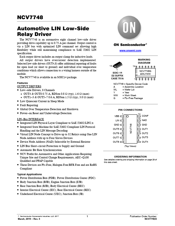
Battery supply input Battery connection 2 LIN LIN bus interface LIN bus pin, low in dominant state 3 GND (Note 1) Ground Ground connection 4 OUT5 LS driver Channel 5 Low-side drive output, Ron = 1.5 W (typ) 5 OUT6 LS driver Channel 6 Low-side drive output, Ron = 1.5 W (typ) 6 OUT7 LS driver Channel 7 Low-side drive output, Ron = 1.5 W (typ) 7 OUT8 LS driver Channel 8 Low-side drive output, Ron = 0.8 W (typ) 8 OUT4 LS driver Channel 4 Low-side drive output, Ron = 0.8 W (typ) 9 OUT3 LS driver Channel 3 Low-side drive output, Ron = 1.5 W (typ) 10 OUT2 LS driver Channel 2 Low-side drive output, Ron = 1.5 W (typ) 11 OUT1 LS driver Channel 1 Low-side drive output, Ron = 1.5 W (typ) 12 GND (Note 1) Ground Ground connection 13 NAD LV analog input/output Node Addressing via external resistor.
Key Features
- Low-side Drivers, 8 Channels
- OUT4 & OUT8 0.75 A, RDSon 0.8 W (typ), 1.6 W (max)
- Low Quiescent Current in Sleep Mode
- Fault Reporting
- Global Over Temperature Detection and Shutdown
- Power-on Reset and Undervoltage Detection LIN-Bus INTERFACE
- Integrated LIN Physical Layer compliant to SAE J2602/LIN2.x
- Integrated State Machine for SAE J2602 compliant LIN Protocol Handling and the LIN Message Decoding
- Virtual LIN Node Concept to Drive up to 32 Relays using One LIN Node Address with up to Four Slaves Devices
- Device Node Address (NAD) Selectable by External Resistor