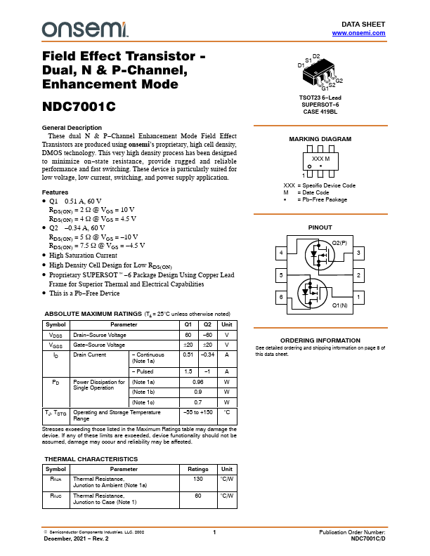
NDC7001C
Description
These dual N & P- Channel Enhancement Mode Field Effect
Transistors are produced using onsemi’s proprietary, high cell density, DMOS technology. This very high density process has been designed to minimize on- state resistance, provide rugged and reliable performance and fast switching. These device is particularly suited for low voltage, low current, switching, and power supply application.
Features
- Q1 0.51 A, 60 V
RDS(ON) = 2 W @ VGS = 10 V RDS(ON) = 4 W @ VGS = 4.5 V
- Q2
- 0.34 A, 60 V
RDS(ON) = 5 W @ VGS =
- 10 V RDS(ON) = 7.5 W @ VGS =
- 4.5 V
- High Saturation Current
- High Density Cell Design for Low RDS(ON)
- Proprietary SUPERSOTt- 6 Package Design Using Copper Lead
Frame for Superior Thermal and Electrical Capabilities
- This is a Pb- Free Device
ABSOLUTE MAXIMUM RATINGS (TA = 25°C unless otherwise noted)
Symbol
Parameter
Q1 Q2 Unit
VDSS VGSS
Drain- Source Voltage
Gate- Source Voltage
Drain Current
- Continuous (Note 1a)
- 60 V ±20 ±20 V 0.51
- 0.34 A
-...