NE5517A
NE5517A is Dual Operational Transconductance Amplifier manufactured by onsemi.
- Part of the NE5517 comparator family.
- Part of the NE5517 comparator family.
Features
- Constant Impedance Buffers
- DVBE of Buffer is Constant with Amplifier IBIAS Change
- Excellent Matching Between Amplifiers
- Linearizing Diodes
- High Output Signal-to-Noise Ratio
- This is a Pb- Free Device
Applications
- Multiplexers
- Timers
- Electronic Music Synthesizers
- Dolby® HX Systems
- Current-Controlled Amplifiers, Filters
- Current-Controlled Oscillators, Impedances
DATA SHEET .onsemi.
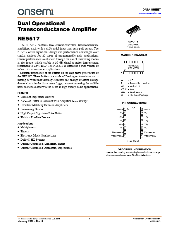
SOIC- 16 D SUFFIX CASE 751B
MARKING DIAGRAM xx5517DG AWLYWW
1 xx = NE A = Assembly Location WL = Wafer Lot YY, Y = Year WW = Work Week G = Pb- Free Package
PIN CONNECTIONS
IABCa 1 Da 2
+INa 3
- INa 4 VOa 5
V- 6
INBUFFERa 7 VOBUFFERa 8
16 IABCb 15 Db 14 +INb 13
- INb 12 VOb 11 V+
10 INBUFFERb 9 VOBUFFERb
(Top View)
ORDERING INFORMATION
See detailed ordering and shipping information in the package dimensions section on page 13 of this data sheet.
© Semiconductor ponents Industries, LLC, 2013
January, 2022
- Rev. 5
Publication Order Number: NE5517/D
PIN DESCRIPTION
Pin...