NL17SH08
NL17SH08 is Single 2-Input AND Gate manufactured by onsemi.
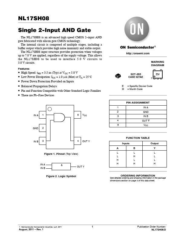
NL17SH08 Single 2-Input AND Gate
The NL17SH08 is an advanced high speed CMOS 2- input AND gate fabricated with silicon gate CMOS technology. The internal circuit is posed of multiple stages, including a buffer output which provides high noise immunity and stable output. The NL17SH08 input structure provides protection when voltages up to 7.0 V are applied, regardless of the supply voltage. This allows the NL17SH08 to be used to interface 5.0 V circuits to 3.0 V circuits.
Features http://onsemi. MARKING DIAGRAM
SOT- 953 CASE 527AE EM 1
- -
- -
- -
High Speed: t PD = 3.5 ns (Typ) at VCC = 5.0 V Low Power Dissipation: ICC = 1.0 m A (Max) at TA = 25°C Power Down Protection Provided on Inputs Balanced Propagation Delays Pin and Function patible with Other Standard Logic Families These are Pb- Free Devices
= Specific Device Code = Month Code
PIN ASSIGNMENT
1 2 IN A 1 5 VCC 3 4 5 GND 2 IN A GND IN B OUT Y VCC
IN B
FUNCTION TABLE
OUT Y A Inputs B L H L H Output Y L L L H
Figure 1. Pinout (Top View)
IN A IN B
&
OUT Y
Figure 2. Logic Symbol
See detailed ordering and shipping information in the package dimensions section on page 4 of this data sheet.
ORDERING INFORMATION
© Semiconductor ponents Industries, LLC, 2011
August, 2011
- Rev. 1
Publication Order Number: NL17SH08/D
MAXIMUM RATINGS
Symbol VCC VIN VOUT IIK IOK IOUT ICC TSTG TL TJ PD MSL FR ILATCHUP DC Supply Voltage DC Input Voltage DC Output Voltage DC Input Diode Current DC Output Diode Current DC Output Sink Current DC Supply Current per Supply Pin Storage Temperature Range Lead Temperature, 1 mm from Case for 10 Seconds Junction Temperature Under Bias Power Dissipation in Still Air Moisture Sensitivity Flammability Rating Latchup Performance Oxygen Index: 28 to 34 Above VCC and Below GND at 125°C (Note 1) Parameter Value
- 0.5 to +7.0
- 0.5 to +7.0
- 0.5 to VCC...