NL3V8T240
Features
- Wide VCCA and VCCB Operating Range: 0.9 V to 3.6 V
- Balanced Output Drive: ±24 m A @ 3.0 V
- High- Speed w/ Balanced Propagation Delay:
2.8 ns max at 3.0 to 3.6 V
- Inputs Pins OVT to 3.6 V
- Non- preferential VCC Sequencing
- Outputs at 3- State until Active VCC is Reached
- Partial Power- Off Protection
- Outputs Switch to 3- State with either VCC at GND
- Typical Max Data Rates:
380 Mbps (≥1.8- V to 3.3- V Translation) 200 Mbps (≥1.1- V to [1.8- V, 2.5- V, 3.3- V] Translation) 150 Mbps (≥1.1- V to 1.5- V Translation) 100 Mbps (≥1.1- V to 1.2- V Translation)
- Small Pb- Free Packaging:
UDFN20, SOIC- 20W, TSSOP- 20
- - Q Suffix for Automotive and Other Applications Requiring Unique
Site and Control Change Requirements; AEC- Q100 Qualified and PPAP Capable-
- These Devices are Pb- Free, Halogen Free/BFR Free and are Ro HS pliant
Typical Applications
- Mobile Phones, PDAs, Other Portable Devices
- Automotive
- Industrial
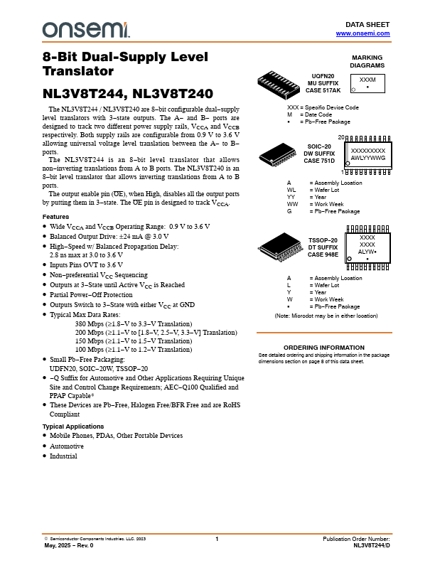
UQFN20 MU SUFFIX CASE 517AK
MARKING DIAGRAMS
XXXM G
XXX = Specific Device...