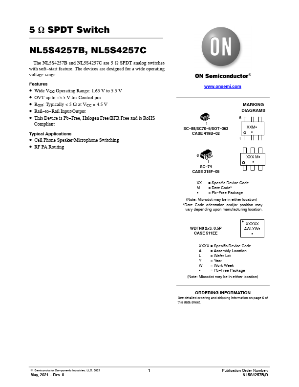
Description
2 NL5S4257B, NL5S4257C Symbol Rating Value Unit VCC Positive DC Supply Voltage -0.5 to +6.0 V VIS Switch Input / Output Voltage -0.5 to VCC+0.5 V VIN Digital Select Input Voltage -0.5 to +6.0 V IOK I/O Port Diode Current ±50 mA IIK Select Input Diode Current -50 mA II/O Continuous DC Current Through Analog Switch ±50 mA II/O-pk Peak Current Through Analog Switch, 10% Duty Cycle ±100 mA Ts Storage Temperature -65 to +150 °C ESD Human Body Model (HBM) 2 kV Stresses exceeding those listed in the REMENDED OPERATING CONDITIONS Symbol Parameter Min Max Unit VCC Positive DC Supply Voltage 1.65 5.5 V VIS Switch Input / Output Voltage GND VCC V VIN Digital Select Input Voltage GND 5.5 V TA Operating Temperature Range -40 +125 °C tr, tf Input Transition Rise or Fall Time VCC v 3.0 V 0 (Select Input IN) VCC > 3.0 V 0 20 ns/V 10 Functional operation above the stresses listed in the Remended Operating Ranges is not implied.
Key Features
- Wide VCC Operating Range: 1.65 V to 5.5 V
- OVT up to +5.5 V for Control pin
- RON: Typically < 5 W at VCC = 4.5 V
- Rail-to-Rail Input/Output
- This Device is Pb-Free, Halogen Free/BFR Free and is RoHS pliant
Applications
- RF PA Routing