NLAS5223C Overview
Key Specifications
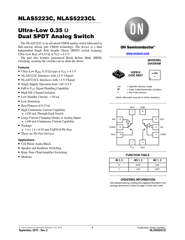
Pins: 10
Operating Voltage: 3 V
Max Voltage (typical range): 4.5 V
Min Voltage (typical range): 1.65 V
Key Features
- Ultra-Low RON, 0.35 W (typ) at VCC = 4.3 V
- NLAS5223C Interfaces with 2.8 V Chipset
- NLAS5223CL Interfaces with 1.8 V Chipset
- Single Supply Operation from 1.65-4.5 V
- Full 0-VCC Signal Handling Capability