NLHV001
NLHV001 is 1-Bit Gate Pulse Modulator manufactured by onsemi.
1-Bit Gate Pulse Modulator
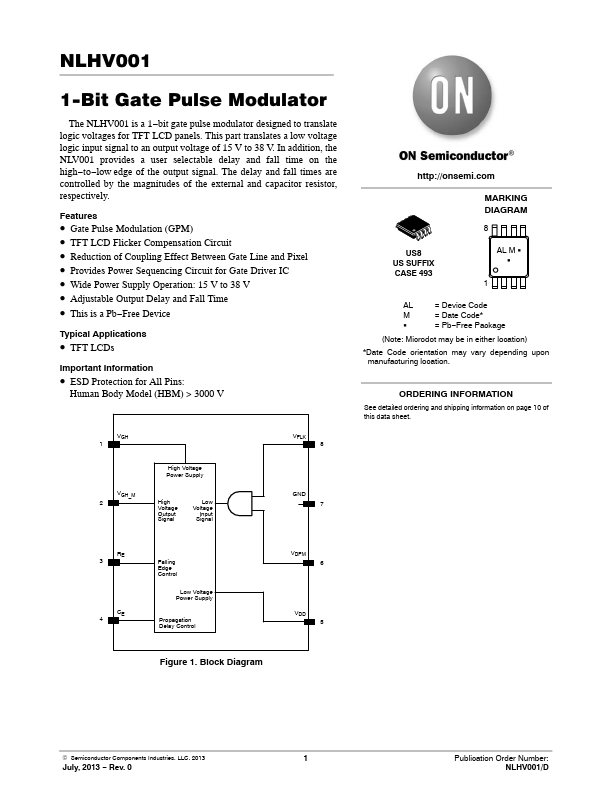
The NLHV001 is a 1- bit gate pulse modulator designed to translate logic voltages for TFT LCD panels. This part translates a low voltage logic input signal to an output voltage of 15 V to 38 V. In addition, the NLV001 provides a user selectable delay and fall time on the high- to- low edge of the output signal. The delay and fall times are controlled by the magnitudes of the external and capacitor resistor, respectively.
Features
- Gate Pulse Modulation (GPM)
- TFT LCD Flicker pensation Circuit
- Reduction of Coupling Effect Between Gate Line and Pixel
- Provides Power Sequencing Circuit for Gate Driver IC
- Wide Power Supply Operation: 15 V to 38 V
-...