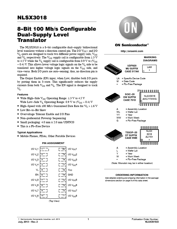
NLSX3018
NLSX3018 is manufactured by onsemi.
8-Bit 100 Mb/s Configurable Dual-Supply Level Translator
The NLSX3018 is a 8- bit configurable dual- supply bidirectional level translator without a direction control pin. The I/O VCC- and I/O VL- ports are designed to track two different power supply rails, VCC and VL respectively. The VCC supply rail is configurable from 1.3 V to 4.5 V while the VL supply rail is configurable from 0.9 V to (VCC
- 0.4) V. This allows lower voltage logic signals on the VL side to be translated into higher voltage logic signals on the VCC side, and vice- versa. Both I/O ports are auto- sensing; thus, no direction pin is required.
The Output Enable (EN) input, when Low, disables both I/O ports by...