NLU3G17
NLU3G17 is Triple Non-Inverting Schmitt-Trigger Buffer manufactured by onsemi.
Triple Non-Inverting Schmitt-Trigger Buffer
The NLU3G17 MiniGatet is an advanced high- speed CMOS triple non- inverting Schmitt- trigger buffer in ultra- small footprint.
The NLU3G17 input and output structures provide protection when voltages up to 7.0 V are applied, regardless of the supply voltage.
The NLU3G17 can be used to enhance noise immunity or to square up slowly changing waveforms.
Features
- High Speed: tPD = 4.0 ns (Typ) @ VCC = 5.0 V
- Low Power Dissipation: ICC = 1 mA (Max) at TA = 25°C
- Power Down Protection Provided on inputs
- Balanced Propagation Delays
- Overvoltage Tolerant (OVT) Input and Output Pins
- Ultra- Small Packages
- These are Pb- Free Devices
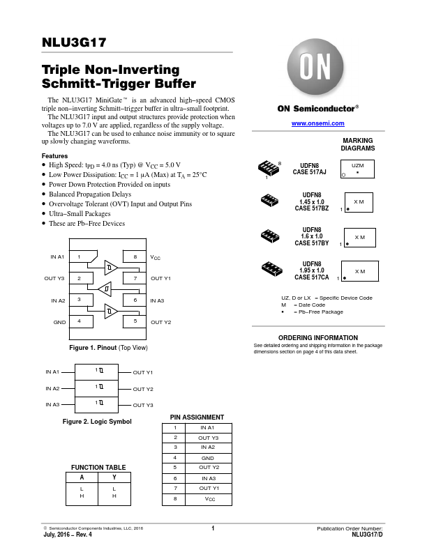
IN A1 1...