NLV74VHC1G09
Features
- Designed for 2.0 V to 5.5 V VCC Operation
- 4.3 ns t PD at 5 V (typ)
- Inputs/Outputs Over- Voltage Tolerant up to 5.5 V
- IOFF Supports Partial Power Down Protection
- Source/Sink 8 m A at 3.0 V
- Available in SC- 88A and TSOP- 5 Packages
- Chip plexity < 100 FETs
- NLV Prefix for Automotive and Other Applications Requiring
Unique Site and Control Change Requirements; AEC- Q100 Qualified and PPAP Capable
- These Devices are Pb- Free, Halogen Free/BFR Free and are Ro HS pliant
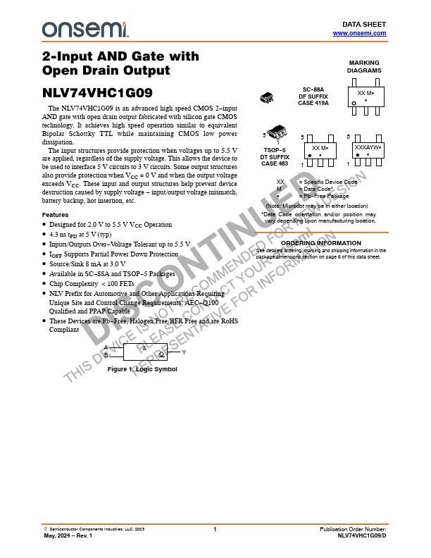
&
Figure 1. Logic Symbol
DATA SHEET .onsemi.
SC- 88A DF SUFFIX CASE 419A
MARKING DIAGRAMS
XX MG G
5 1
TSOP- 5 DT SUFFIX CASE 483
XX MG G
XXXAYWG G
= Specific Device Code
= Date Code-
= Pb- Free Package
(Note: Microdot may be in either location)
- Date Code orientation and/or position may vary depending upon manufacturing location.
ORDERING INFORMATION
See detailed ordering, marking and shipping information in the package dimensions section on page 6 of this data sheet.
©...