NLVHC1G66
NLVHC1G66 is SPST (NO) Normally Open Analog Switch manufactured by onsemi.
MC74VHC1G66, NLVHC1G66 SPST (NO) Normally Open Analog Switch
The MC74VHC1G66, NLVHC1G66 is a single pole single throw (SPST) analog switch. It achieves high speed propagation delays and low ON resistances while maintaining low power dissipation. This bilateral switch controls analog and digital voltages that may vary across the full power- supply range (from VCC to GND). The MC74VHC1G66, NLVHC1G66 is patible in function to a single gate of the High Speed CMOS MC74VHC4066 and the metal- gate CMOS MC14066. The device has been designed so that the ON resistances (RON) are much lower and more linear over input voltage than RON of the metal- gate CMOS or High Speed CMOS analog switches. The newer NLVHC offers the same functionality in a 1.2x1.0x0.55mm UDFN6 package. The ON/OFF control inputs are patible with standard CMOS outputs. The ON/OFF control input structure provides protection when voltages between 0 V and 5.5 V are applied, regardless of the supply voltage. This input structure helps prevent device destruction caused by supply voltage
- input/output voltage mismatch, battery backup, hot insertion, etc.
Features
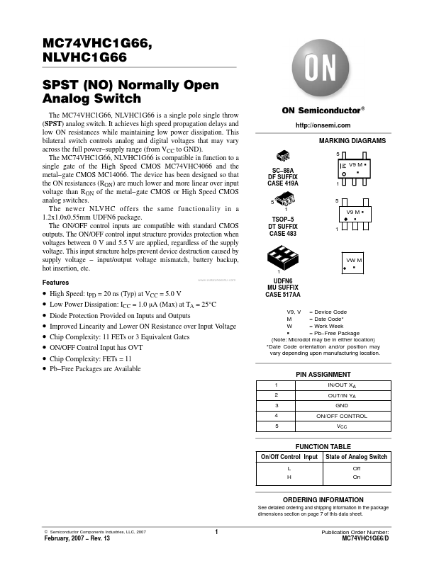
.. http://onsemi. MARKING DIAGRAMS
5 SC- 88A DF SUFFIX CASE 419A 5 1 TSOP- 5 DT SUFFIX CASE 483 V9 M G G M 1 5 V9 M G G 1
1 UDFN6 MU SUFFIX CASE 517AA
VW M G
- -
- -
- -
- -
High Speed: t PD = 20 ns (Typ) at VCC = 5.0 V Low Power Dissipation: ICC = 1.0 m A (Max) at TA = 25°C Diode Protection Provided on Inputs and Outputs Improved Linearity and Lower ON Resistance over Input Voltage Chip plexity: 11 FETs or 3 Equivalent Gates ON/OFF Control Input has OVT Chip plexity: FETs = 11 Pb- Free Packages are Available
V9, V = Device Code M = Date Code- W = Work Week G = Pb- Free Package (Note: Microdot may be in either location)
- Date Code orientation and/or position may vary depending upon manufacturing location.
PIN ASSIGNMENT
1 2 3 4 5 IN/OUT XA OUT/IN YA GND ON/OFF CONTROL VCC
FUNCTION TABLE
On/Off Control Input L H State of...