NLX1G332
NLX1G332 is 3-Input OR Gate manufactured by onsemi.
3-Input OR Gate
The NLX1G332 is an advanced high- speed 3- input CMOS OR gate in ultra- small footprint.
The NLX1G332 input structures provide protection when voltages up to 7.0 V are applied, regardless of the supply voltage.
Features
- High Speed: tPD = 2.4 ns (Typ) @ VCC = 5.0 V
- Designed for 1.65 V to 5.5 V VCC Operation
- Low Power Dissipation: ICC = 1 mA (Max) at TA = 25°C
- 24 mA Balanced Output Source and Sink Capability
- Balanced Propagation Delays
- Overvoltage Tolerant (OVT) Input Pins
- Ultra- Small Packages
- These are Pb- Free Devices
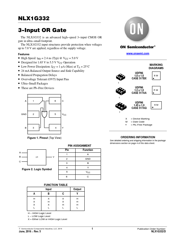
6C
4Y
.onsemi.
MARKING DIAGRAMS
UDFN6
1.0 x 1.0
6M
CASE 517BX
UDFN6
1.2 x 1.0
CASE...