NSS20600CF8T1G
NSS20600CF8T1G is Low VCE(sat) PNP Transistor manufactured by onsemi.
..
NSS20600CF8T1G 20 V, 7.0 A, Low VCE(sat) PNP Transistor
ON Semiconductor’s e2 Power Edge family of low VCE(sat) transistors are miniature surface mount devices featuring ultra low saturation voltage (VCE(sat)) and high current gain capability. These are designed for use in low voltage, high speed switching applications where affordable efficient energy control is important. Typical applications are DC- DC converters and power management in portable and battery powered products such as cellular and cordless phones, PDAs, puters, printers, digital cameras and MP3 players. Other applications are low voltage motor controls in mass storage products such as disc drives and tape drives. In the automotive industry they can be used in air bag deployment and in the instrument cluster. The high current gain allows e2Power Edge devices to be driven directly from PMU’s control outputs, and the Linear Gain (Beta) makes them ideal ponents in analog amplifiers.
- This is a Pb- Free Device
MAXIMUM RATINGS (TA = 25°C)
Rating Collector-Emitter Voltage Collector-Base Voltage Emitter-Base Voltage Collector Current
- Continuous Collector Current
- Peak Electrostatic Discharge Symbol VCEO VCBO VEBO IC ICM ESD Max
- 20
- 20
- 7.0
- 6.0
- 7.0 Unit Vdc Vdc Vdc Adc A http://onsemi.
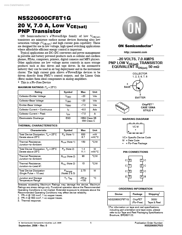
- 20 VOLTS, 7.0 AMPS PNP LOW VCE(sat) TRANSISTOR EQUIVALENT RDS(on) 50 m W
COLLECTOR 1, 2, 3, 6, 7, 8 4 BASE 5 EMITTER Chip FET] CASE 1206A STYLE 4
HBM Class 3B MM Class C
MARKING DIAGRAM
VC M G VC = Specific Device Code M = Date Code G = Pb- Free Package
THERMAL CHARACTERISTICS
Characteristic Total Device Dissipation, TA = 25°C Derate above 25°C Thermal Resistance, Junction- to- Ambient Total Device Dissipation, TA = 25°C Derate above 25°C Thermal Resistance, Junction- to- Ambient Thermal Resistance, Junction- to- Lead #1 Total Device Dissipation (Single Pulse < 10 sec) Junction and Storage Temperature Range Symbol PD (Note 1) Rq JA (Note 1) PD (Note 2) Rq JA (Note 2) Rq JL (Note 2) PDsingle (Notes 2 & 3) TJ, Tstg Max 830...