NSVB1706DMW5T1G
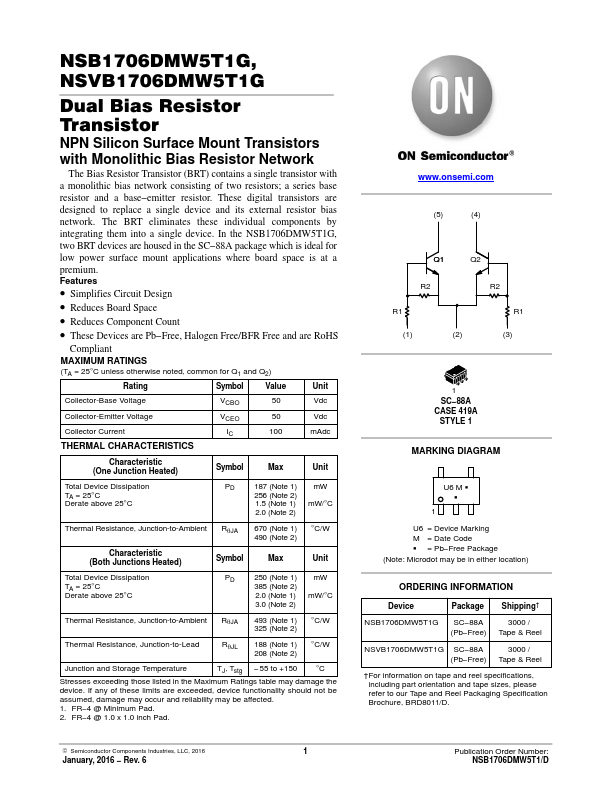
Features
- Simplifies Circuit Design
- Reduces Board Space
- Reduces ponent Count
- These Devices are Pb- Free, Halogen Free/BFR Free and are Ro HS pliant
MAXIMUM RATINGS (TA = 25°C unless otherwise noted, mon for Q1 and Q2)
Rating
Symbol
Value
Unit
Collector-Base Voltage
VCBO
Vdc
Collector-Emitter Voltage
VCEO
Vdc
Collector Current
100 m Adc
THERMAL CHARACTERISTICS
Characteristic (One Junction Heated)
Symbol
Max
Unit
Total Device Dissipation TA = 25°C Derate above 25°C
PD 187 (Note 1) m W 256 (Note 2)
1.5 (Note 1) m W/°C
2.0 (Note 2)
Thermal Resistance, Junction-to-Ambient Rq JA
670 (Note 1) °C/W 490 (Note 2)
Characteristic (Both Junctions Heated)
Symbol
Max
Unit
Total Device Dissipation TA = 25°C Derate above 25°C
PD 250 (Note 1) m W 385 (Note 2)
2.0 (Note 1) m W/°C
3.0 (Note...