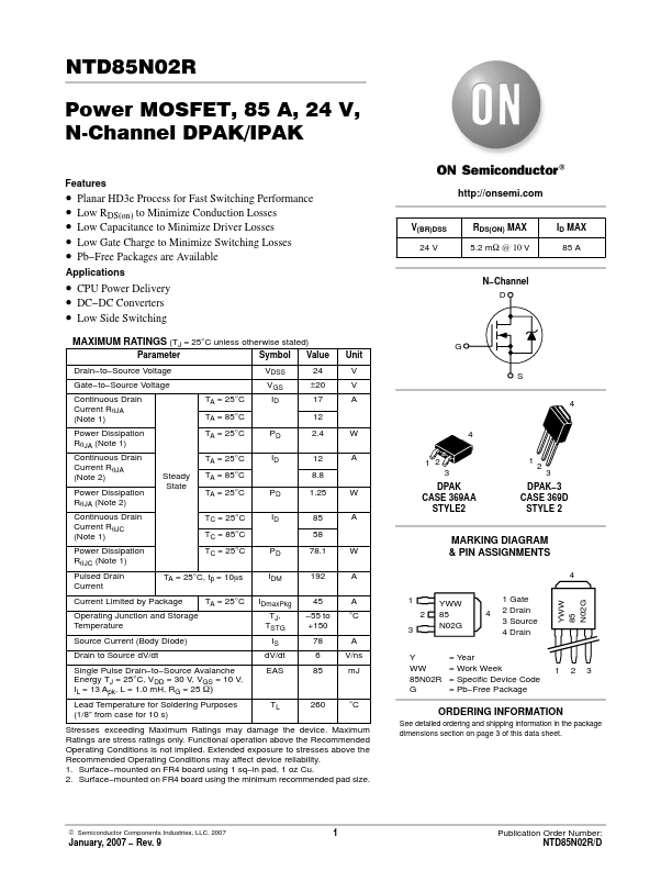
Full PDF Text Transcription for NTD85N02R (Reference)
Note: Below is a high-fidelity text extraction (approx. 800 characters) for
NTD85N02R. For precise diagrams, and layout, please refer to the original PDF.
NTD85N02R Power MOSFET, 85 A, 24 V, N-Channel DPAK/IPAK Features • Planar HD3e Process for Fast Switching Performance • Low RDS(on) to Minimize Conduction Losses • Low Ca...
View more extracted text
ching Performance • Low RDS(on) to Minimize Conduction Losses • Low Capacitance to Minimize Driver Losses • Low Gate Charge to Minimize Switching Losses • Pb−Free Packages are Available Applications • CPU Power Delivery • DC−DC Converters • Low Side Switching MAXIMUM RATINGS (TJ = 25°C unless otherwise stated) Parameter Symbol Value Unit Drain−to−Source Voltage Gate−to−Source Voltage Continuous Drain Current RqJA (Note 1) VDSS 24 V VGS ±20 V TA = 25°C ID 17 A TA = 85°C 12 Power Dissipation RqJA (Note 1) TA = 25°C PD Continuous Drain TA = 25°C ID Current RqJA (Note 2) Steady TA = 85°C State Power Dissipation TA = 25°C PD Rq