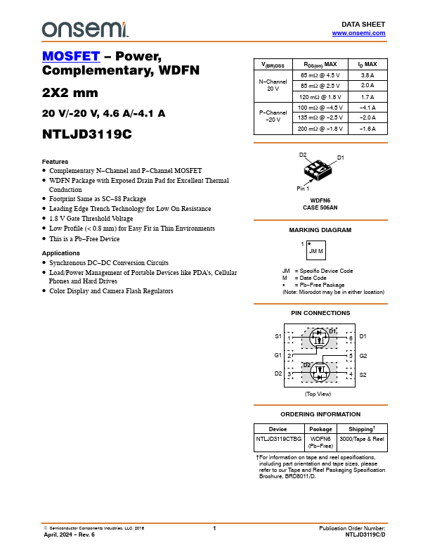
Datasheet4U Logo Datasheet4U.com

NTLJD3119C - Power MOSFET

Key Features

  • Complementary N.
  • Channel and P.
  • Channel MOSFET.
  • WDFN Package with Exposed Drain Pad for Excellent Thermal Conduction.
  • Footprint Same as SC.
  • 88 Package.
  • Leading Edge Trench Technology for Low On Resistance.
  • 1.8 V Gate Threshold Voltage.
  • Low Profile (< 0.8 mm) for Easy Fit in Thin Environments.
  • This is a Pb.
  • Free Device.

📥 Download Datasheet

Full PDF Text Transcription (Reference)

The following content is an automatically extracted verbatim text from the original manufacturer datasheet and is provided for reference purposes only.

View original datasheet text
MOSFET – Power, Complementary, WDFN 2X2 mm 20 V/-20 V, 4.6 A/-4.1 A NTLJD3119C Features • Complementary N−Channel and P−Channel MOSFET • WDFN Package with Exposed Drain Pad for Excellent Thermal Conduction • Footprint Same as SC−88 Package • Leading Edge Trench Technology for Low On Resistance • 1.8 V Gate Threshold Voltage • Low Profile (< 0.8 mm) for Easy Fit in Thin Environments • This is a Pb−Free Device Applications • Synchronous DC−DC Conversion Circuits • Load/Power Management of Portable Devices like PDA’s, Cellular Phones and Hard Drives • Color Display and Camera Flash Regulators DATA SHEET www.onsemi.com V(BR)DSS N−Channel 20 V P−Channel −20 V RDS(on) MAX 65 mW @ 4.5 V 85 mW @ 2.5 V 120 mW @ 1.8 V 100 mW @ −4.5 V 135 mW @ −2.5 V 200 mW @ −1.8 V ID MAX 3.8 A 2.0 A 1.7 A −4.