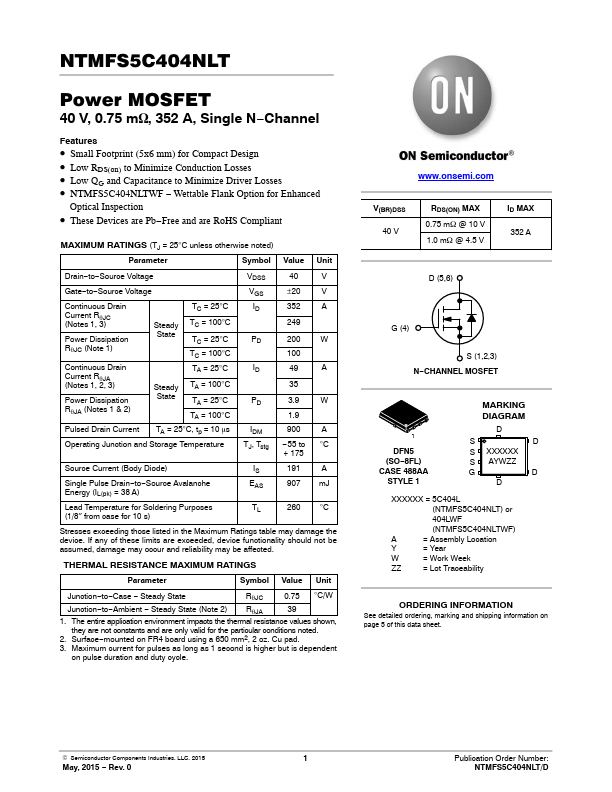
NTMFS5C404NLT
Features
- Small Footprint (5x6 mm) for pact Design
- Low RDS(on) to Minimize Conduction Losses
- Low QG and Capacitance to Minimize Driver Losses
- NTMFS5C404NLTWF
- Wettable Flank Option for Enhanced
Optical Inspection
- These Devices are Pb- Free and are Ro HS pliant
MAXIMUM RATINGS (TJ = 25°C unless otherwise noted)
Parameter
Symbol Value
Unit
Drain- to- Source Voltage
Gate- to- Source Voltage
Continuous Drain C(Nuortreesnt1R, 3q J)C Power Dissipation Rq JC (Note 1)
Steady State
TC = 25°C TC = 100°C TC = 25°C TC = 100°C
Continuous Drain C(Nuortreesnt1R, 2q J,A3) Power Dissipation Rq JA (Notes 1 & 2)
Steady State
TA = 25°C TA = 100°C TA = 25°C TA = 100°C
Pulsed Drain Current TA = 25°C, tp = 10 ms
Operating Junction and Storage Temperature
VDSS VGS ID
IDM TJ, Tstg
40 ±20 352 249 200 100 49 35 3.9 1.9 900
- 55 to + 175
A °C
Source Current (Body Diode)
IS 191 A
Single Pulse Drain- to- Source Avalanche Energy (IL(pk) = 38 A)
EAS 907 m J
Lead Temperature for...