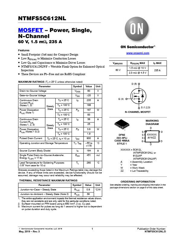
NTMFS5C612NL
Features
- Small Footprint (5x6 mm) for pact Design
- Low RDS(on) to Minimize Conduction Losses
- Low QG and Capacitance to Minimize Driver Losses
- NTMFS5C612NLWF
- Wettable Flank Option for Enhanced Optical
Inspection
- These Devices are Pb- Free and are Ro HS pliant
.onsemi.
V(BR)DSS 60 V
RDS(ON) MAX 1.5 m W @ 10 V 2.3 m W @ 4.5 V
ID MAX 235 A
MAXIMUM RATINGS (TJ = 25°C unless otherwise noted)
Parameter
Symbol Value Unit
Drain- to- Source Voltage
VDSS
Gate- to- Source Voltage
±20
Continuous Drain Current Rq JC (Notes 1, 3)
Power Dissipation Rq JC (Note 1)
TC = 25°C
Steady TC = 100°C
State TC = 25°C
TC = 100°C
167 W
Continuous Drain Current Rq JA (Notes 1, 2, 3)
Power Dissipation Rq JA (Notes 1 & 2)
TA = 25°C
Steady TA = 100°C
State TA =...