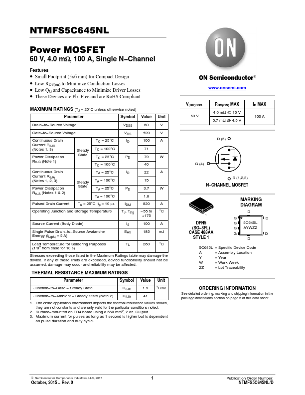
NTMFS5C645NL
Features
- Small Footprint (5x6 mm) for pact Design
- Low RDS(on) to Minimize Conduction Losses
- Low QG and Capacitance to Minimize Driver Losses
- These Devices are Pb- Free and are Ro HS pliant
MAXIMUM RATINGS (TJ = 25°C unless otherwise noted)
Parameter
Symbol Value Unit
Drain- to- Source Voltage
Gate- to- Source Voltage
Continuous Drain Current Rq JC (Notes 1, 3)
Power Dissipation Rq JC (Note 1)
Steady State
TC = 25°C TC = 100°C TC = 25°C TC = 100°C
Continuous Drain Current Rq JA (Notes 1, 2, 3)
Power Dissipation Rq JA (Notes 1 & 2)
Steady State
TA = 25°C TA = 100°C TA = 25°C TA = 100°C
Pulsed Drain Current TA = 25°C, tp = 10 ms
Operating Junction and Storage Temperature
VDSS VGS ID
IDM TJ, Tstg
60 ±20 100 71 79 40 22 15 3.7 1.8 820
- 55 to +175
A °C
Source Current (Body Diode)
Single Pulse Drain- to- Source Avalanche Energy (IL(pk) = 5 A)
Lead Temperature for Soldering Purposes (1/8″ from case for 10 s)
IS 100 A EAS 185 m J
TL 260 °C
Stresses exceeding...