NUD4301
NUD4301 is Dual Low Dropout Voltage LED Driver/Current Source manufactured by onsemi.
Features http://onsemi.
MARKING DIAGRAM
43 M G G 1 DFN8 CASE 506AQ 43 M G = Specific Device Code = Date Code = Pb- Free Package
- -
- -
- -
Ultra Low Dropout Voltage < 200 m V Programmable Output Current from 1 m A to 30 m A Dual Output with Independent Current Limit Set DC Current in LED Analog/Digital PWM Capability This is a Pb- Free Device
(Note: Microdot may be in either location)
PIN CONFIGURATION
1 2 3 4
Typical Applications
- Portables: PDAs, Cell phones
- Li- Ion Battery Applications
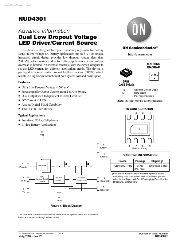
9 9 Vcc
6 Drain1 7 Drain2
7 6 5 (Bottom View)
1 Enable
2 Dim 3 NC
ÎÎÎÎ ÎÎÎÎ ÎÎÎÎ ÎÎÎ ÎÎÎ ÎÎÎÎÎÎÎ ÎÎÎ
Enable
PWM Analog/ Digital Control Current Limit FET1 Current Limit FET2
ORDERING INFORMATION
Device NUD4301MNT1G Package DFN8 (Pb- Free) Shipping † 3000/Tape & Reel
†For information on tape and reel specifications, including part orientation and tape sizes, please 8 refer to our Tape and Reel Packaging Specification Source2 Brochure, BRD8011/D. 5 Source1
4 Gnd
Figure 1. Block Diagram
This document contains information on a new product. Specifications and information herein are subject to change without notice.
© Semiconductor ponents Industries, LLC, 2006
July, 2006
- Rev. P3
Publication Order Number: NUD4301/D
FUNCTIONAL PIN DESCRIPTIONS
Pin 1 2 3 4 5 6 7 8 9 Function Enable Dim N.C. Gnd Source1 Drain1 Drain2 Source2 Vcc Description
The device is enabled with a positive voltage signal at this pin. The enable controls both channels. This pin is used for analog or PWM dimming control. An analog signal of 0
- 3.3 volts is required, or a PWM signal with an amplitude greater than 3.3 volts. The dim controls both channels. No connection. Ground Reference to the device. Source terminal of the FET 1 Drain terminal of the FET 1, which is also the switching node of the load 1. Drain terminal of the FET 2, which is also the switching node of the load 2. Source terminal of the FET 2 Input voltage to the LED driver. This voltage is patible with any battery based...