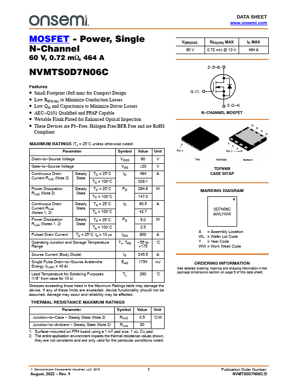
NVMTS0D7N06C
Features
- Small Footprint (8x8 mm) for pact Design
- Low RDS(on) to Minimize Conduction Losses
- Low QG and Capacitance to Minimize Driver Losses
- AEC- Q101 Qualified and PPAP Capable
- Wettable Flank Plated for Enhanced Optical Inspection
- These Devices are Pb- Free, Halogen Free/BFR Free and are Ro HS pliant
MAXIMUM RATINGS (TJ = 25°C unless otherwise noted)
Parameter
Symbol Value Unit
Drain- to- Source Voltage
VDSS
Gate- to- Source Voltage
±20
Continuous Drain
Steady TC = 25°C
Current Rq JC (Note 2) State TC = 100°C
Power Dissipation Rq JC (Note 2)
Steady TC = 25°C
State
TC = 100°C
294.6 W 147.3
Continuous Drain Current Rq JA (Notes 1, 2)
Steady TA = 25°C
State
TA = 100°C
60.5 A 42.7
Power Dissipation Rq JA (Notes 1, 2)
Steady TA = 25°C
State
TA =...