NXV65HR82DS2
NXV65HR82DS2 is DC-DC Converter manufactured by onsemi.
- Part of the NXV65HR82DS1 comparator family.
- Part of the NXV65HR82DS1 comparator family.
Features
- SIP or DIP H- Bridge Power Module for On- board Charger (OBC) in
EV or PHEV
- 5 k V/1 s Electrically Isolated Substrate for Easy Assembly
- Creepage and Clearance per IEC60664- 1, IEC 60950- 1
- pact Design for Low Total Module Resistance
- Module Serialization for Full Traceability
- Lead Free, Ro HS and UL94V- 0 pliant
- Automotive Qualified per AEC Q101 and AQG324 Guidelines
Applications
- DC- DC Converter for On- board Charger in EV or PHEV
Benefits
- Enable Design of Small, Efficient and Reliable System for Reduced
Vehicle Fuel Consumption and CO2 Emission
- Simplified Assembly, Optimized Layout, High Level of Integration, and Improved Thermal Performance
.onsemi.
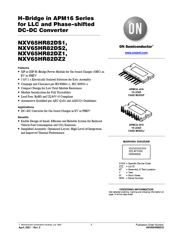
APMCA- A16 16 LEAD
CASE MODGF
APMCA- B16 16 LEAD
CASE MODGJ
MARKING DIAGRAM XXXXXXXXXXX ZZZ ATYWW NNNNNNN
XXXX = Specific Device Code ZZZ = Lot ID AT = Assembly & Test Location Y = Year W = Work Week NNN = Serial Number
ORDERING INFORMATION
See detailed ordering, marking and shipping information on page 10 of this data sheet.
© Semiconductor ponents Industries, LLC, 2020
April, 2021
- Rev. 2
Publication Order Number: NXV65HR82D/D
NXV65HR82DS1, NXV65HR82DS2, NXV65HR82DZ1, NXV65HR82DZ2
Pin Configuration and Block Diagram
Figure 1. Pin Configuration
Table 1. PIN DESCRIPTION
Pin Number
Pin Name
1, 2
AC1
Q1...