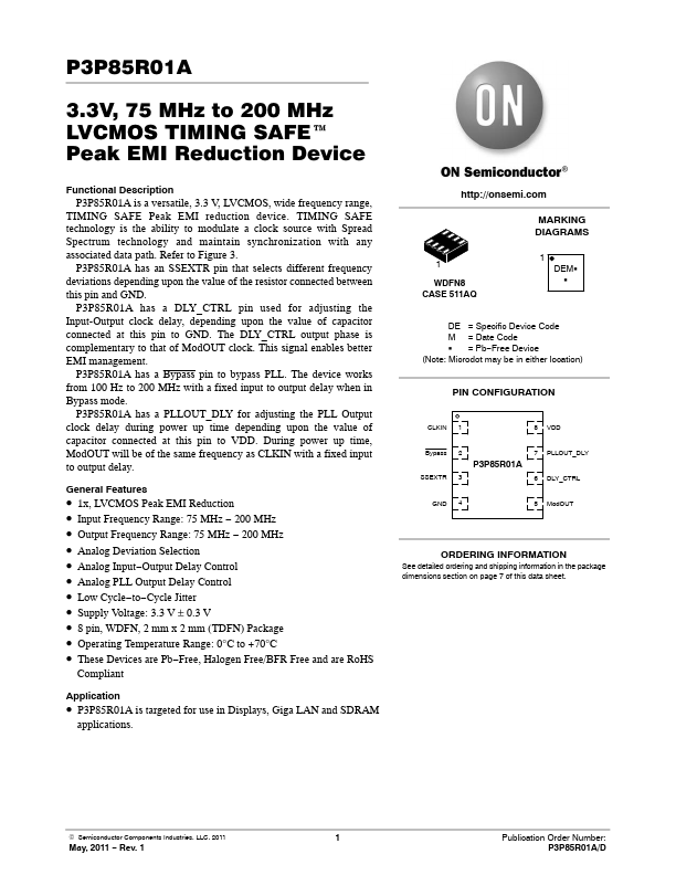
P3P85R01A Overview
Key Features
- 1x, LVCMOS Peak EMI Reduction
- Input Frequency Range: 75 MHz
- Output Frequency Range: 75 MHz
- Analog Deviation Selection
- Analog Input-Output Delay Control
- Analog PLL Output Delay Control
- Low Cycle-to-Cycle Jitter
- Supply Voltage: 3.3 V ± 0.3 V
- 8 pin, WDFN, 2 mm x 2 mm (TDFN) Package
- Operating Temperature Range: 0°C to +70°C