PCS3P623Z09B
PCS3P623Z09B is Peak EMI Reduction IC manufactured by onsemi.
- Part of the PCS3P623Z05A comparator family.
- Part of the PCS3P623Z05A comparator family.
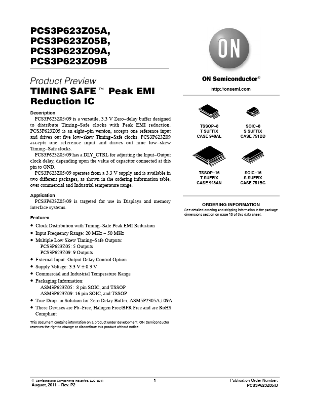
PCS3P623Z05A, PCS3P623Z05B, PCS3P623Z09A, PCS3P623Z09B
Product Preview
TIMING SAFEt Peak EMI
Reduction IC
Description PCS3P623Z05/09 is a versatile, 3.3 V Zero- delay buffer designed to distribute Timing- Safe clocks with Peak EMI reduction. PCS3P623Z05 is an eight- pin version, accepts one reference input and drives out five low- skew Timing- Safe clocks. PCS3P623Z09 accepts one reference input and drives out nine low- skew Timing- Safe clocks.
PCS3P623Z05/09 has a DLY_CTRL for adjusting the Input- Output clock delay, depending upon the value of capacitor connected at this pin to GND.
PCS3P623Z05/09 operates from a 3.3 V supply and is available in two different packages, as shown in the ordering...