PCS3P73Z01AW
Description
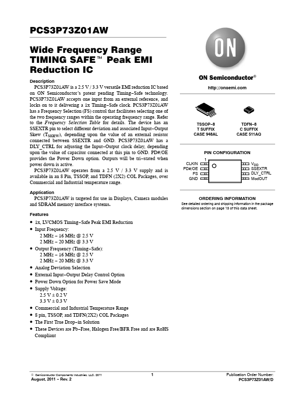
PCS3P73Z01AW is a 2.5 V / 3.3 V versatile EMI reduction IC based on ON Semiconductor’s patent pending Timing−Safe technology.
Key Features
- 1x, LVCMOS Timing−Safe Peak EMI Reduction
- Input Frequency
- Output Frequency (Timing−Safe)
- Analog Deviation Selection
- External Input−Output Delay Control Option
- Power Down Option for Power Save Mode
- Supply Voltage
- mercial and Industrial Temperature Range
- 8 pin, TSSOP, and TDFN(2X2) COL Packages
- The First True Drop−in Solution