PCS3P8504A
PCS3P8504A is General Purpose Peak EMI Reduction IC manufactured by onsemi.
PCS3P8504A General Purpose Peak EMI Reduction IC
Functional Description
.. http://onsemi. MARKING DIAGRAMS
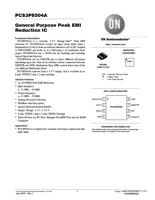
1 WDFN8 CASE 511AQ 1
PCS3P8504A is a versatile, 3.3 V Timing-Safe Peak EMI reduction IC. PCS3P8504A accepts an input clock either from a fundamental Crystal or from an external reference (AC or DC coupled to XIN/CLKIN) and locks on to it delivering a 1x modulated clock output. PCS3P8504A has a SSON pin for enabling and disabling Spread Spectrum function. PCS3P8504A has an SSEXTR pin to select different deviations depending upon the value of an external resistor connected between SSEXTR and GND. Modulation Rate (MR) control selects one of the two different Modulation Rates. PCS3P8504A operates from a 3.3 V supply, and is available in an 8-pin, WDFN(2 mm x 2 mm) package.
General Features
DAMG G
DA = Specific Device Code M = Date Code G = Pb--Free Device
- 1x, LVCMOS Peak EMI Reduction
- Input frequency:
- -
- -
- -
- 15 MHz
- 50 MHz Output frequency: 15 MHz
- 50 MHz Analog Deviation Selection Mod Rate selection option Spread Spectrum Enable/Disable Supply Voltage: 3.3 V ± 0.3 V 8-pin, WDFN 2 mm x 2 mm (TDFN) Package These Devices are Pb-Free, Halogen Free/BFR Free and are Ro HS pliant
PIN CONFIGURATION
XIN/CLKIN 1 XOUT 2 SSON 3 GND 4 8 7 6 5 VDD SSEXTR MR Mod OUT
Application
- PCS3P8504A is targeted for consumer electronics application like
DPF, MFP.
ORDERING INFORMATION
See detailed ordering and shipping information in the package dimensions section on page 5 of this data sheet.
Semiconductor ponents Industries, LLC, 2010
July, 2010
- Rev. 1
Publication Order Number: PCS3P8504A/D
SSON MR VDD
XIN/CLKIN XOUT Crystal Oscillator Mod OUT...