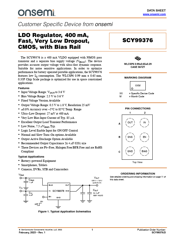
| Part | SCY99376 |
|---|---|
| Description | LDO Regulator |
| Category | LDO Regulator |
| Manufacturer | onsemi |
| Size | 0.98 MB |
Related Datasheets
| Part Number | Manufacturer | Description |
|---|---|---|
| LM317 | Texas Instruments | 3-Terminal Adjustable Regulator |
| TL431 | Fairchild Semiconductor | Programmable Shunt Regulator |
| LM317 | Inchange Semiconductor | Adjustable Voltage Regulator |
