SMMBF4391LT1G Overview
Key Specifications
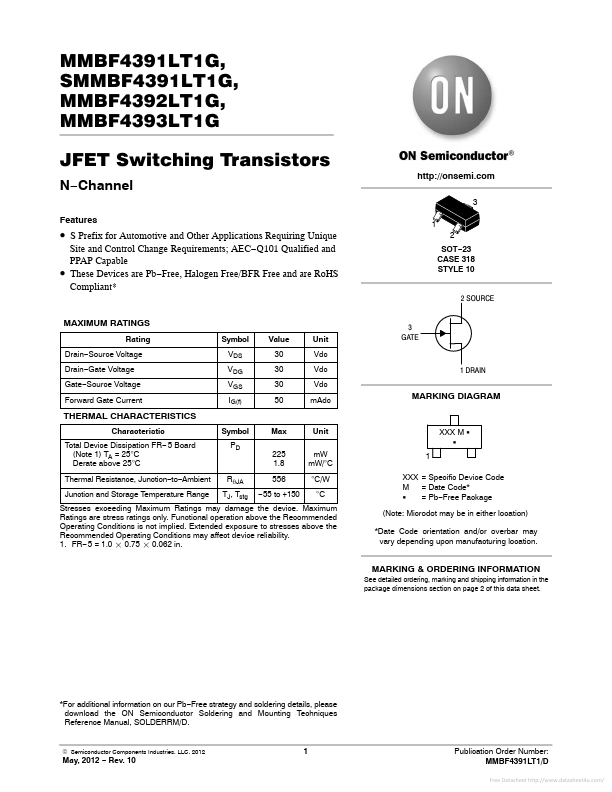
Package: SOT-23-3
Pins: 3
Max Operating Temp: 150 °C
Min Operating Temp: -55 °C
Key Features
- S Prefix for Automotive and Other Applications Requiring Unique
| Part | SMMBF4391LT1G |
|---|---|
| Description | JFET Switching Transistors |
| Category | Transistor |
| Manufacturer | onsemi |
| Size | 154.38 KB |
Package: SOT-23-3
Pins: 3
Max Operating Temp: 150 °C
Min Operating Temp: -55 °C
| Seller | Inventory | Price Breaks | Buy |
|---|---|---|---|
| Verical | 30201 | 1244+ : 0.3015 USD 10000+ : 0.2688 USD 100000+ : 0.2253 USD |
View Offer |
| Rochester Electronics | 30201 | 100+ : 0.2906 USD 500+ : 0.2615 USD 1000+ : 0.2412 USD 10000+ : 0.215 USD |
View Offer |
| Part Number | Manufacturer | Description |
|---|---|---|
| BD777 | Motorola Semiconductor | Plastic Darlington Complementary Silicon Power Transistors |
| D718 | SavantIC | Silicon NPN Power Transistors |
| C33725 | onsemi | Amplifier Transistors |