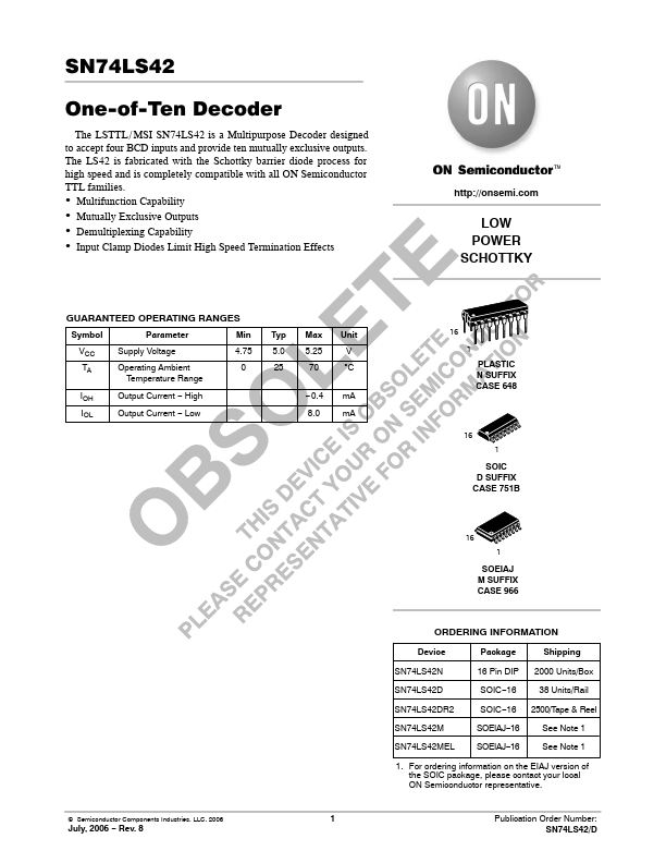
SN74LS42 Overview
Key Specifications
Package: SOP
Mount Type: Surface Mount
Pins: 16
Operating Voltage: 5 V
Key Features
- Multifunction Capability
- Mutually Exclusive Outputs
| Part | SN74LS42 |
|---|---|
| Description | 1-of-10 Decoder |
| Manufacturer | onsemi |
| Size | 203.55 KB |
Package: SOP
Mount Type: Surface Mount
Pins: 16
Operating Voltage: 5 V
| Seller | Inventory | Price Breaks | Buy |
|---|---|---|---|
| Rochester Electronics | 3800 | 25+ : 2.4 USD 100+ : 2.28 USD 500+ : 2.16 USD 1000+ : 2.04 USD |
View Offer |
| Verical | 3800 | 132+ : 2.85 USD 500+ : 2.7 USD 1000+ : 2.55 USD 10000+ : 2.4 USD |
View Offer |
| Part Number | Manufacturer | Description |
|---|---|---|
| SN74LS42 | Motorola Semiconductor | ONE-OF-TEN DECODER |
| SN74LS42 | Texas Instruments | 4-LINE BCD TO 10-LINE DECIMAL DECODERS |
| SN74LS422 | Texas Instruments | Retriggerable Monostable Multivibrator |
| SN74LS423 | Texas Instruments | Retriggerable Monostable Multivibrator |
| SN74LS47D | Texas Instruments | BCD-TO-SEVEN-SEGMENT DECODERS/DRIVERS |