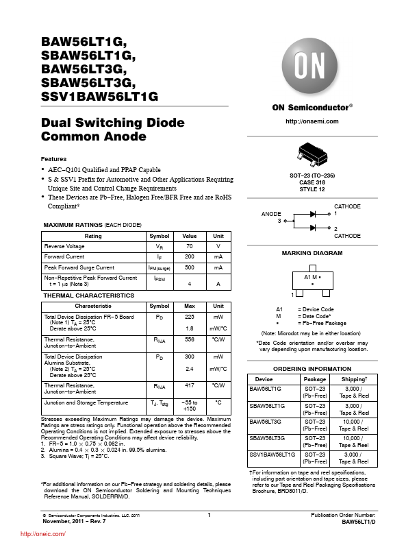
SSV1BAW56LT1G
SSV1BAW56LT1G is Dual Switching Diode Common Anode manufactured by onsemi.
Features
- AEC- Q101 Qualified and PPAP Capable
- S & SSV1 Prefix for Automotive and Other Applications Requiring
Unique Site and Control Change Requirements
- These Devices are Pb- Free, Halogen Free/BFR Free and are Ro HS pliant-
MAXIMUM RATINGS (EACH DIODE)
Rating
Symbol Value
Unit
Reverse Voltage Forward Current Peak Forward Surge Current Non- Repetitive Peak Forward Current t = 1 ms (Note 3)
VR IF IFM(surge) IFSM
70 200 500
V m A m A
THERMAL CHARACTERISTICS
Characteristic
Symbol
Max
Unit
Total Device Dissipation FR- 5 Board PD 225 m W
(Note 1) TA = 25C
Derate above 25C
1.8 m W/C
Thermal Resistance, Junction- to- Ambient
Rq JA
556 C/W
Total Device Dissipation Alumina Substrate,
(Note 2) TA = 25C Derate above 25C
PD 300 m W 2.4 m W/C
Thermal Resistance, Junction- to- Ambient
Rq JA
417 C/W
Junction and Storage Temperature
TJ, Tstg
- 55 to +150
C
Stresses exceeding Maximum Ratings may damage the device. Maximum Ratings are stress ratings only. Functional operation above the Remended Operating Conditions is not implied. Extended exposure to stresses above the Remended Operating Conditions may affect device reliability. 1. FR- 5 = 1.0 0.75 0.062 in. 2. Alumina = 0.4 0.3 0.024 in. 99.5% alumina. 3. Square Wave; Tj = 25C.
- For additional information on our Pb- Free strategy and soldering details, please download the ON Semiconductor Soldering and Mounting Techniques Reference Manual, SOLDERRM/D.
Semiconductor ponents Industries, LLC,...