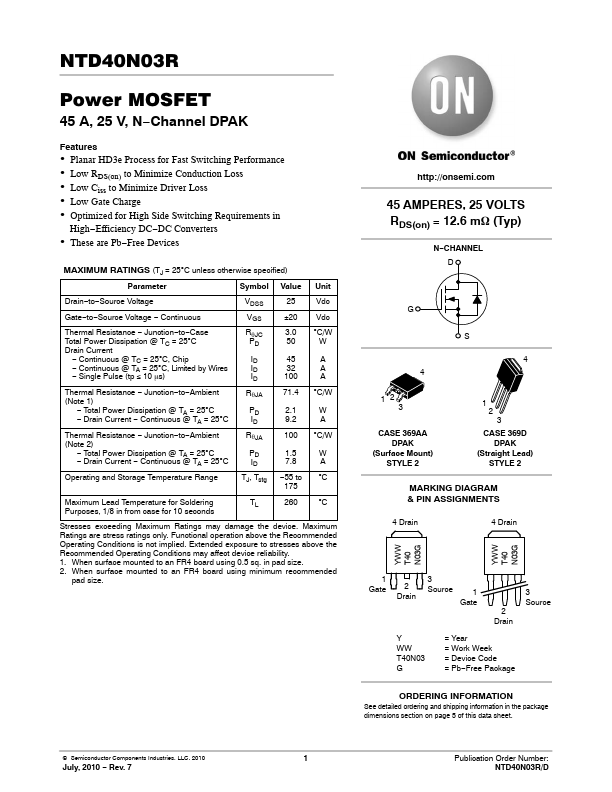
Click to expand full text
NTD40N03R
Power MOSFET
45 A, 25 V, N−Channel DPAK
Features
• Planar HD3e Process for Fast Switching Performance • Low RDS(on) to Minimize Conduction Loss • Low Ciss to Minimize Driver Loss • Low Gate Charge • Optimized for High Side Switching Requirements in
High−Efficiency DC−DC Converters
• These are Pb−Free Devices
MAXIMUM RATINGS (TJ = 25°C unless otherwise specified)
Parameter
Symbol Value
Unit
Drain−to−Source Voltage Gate−to−Source Voltage − Continuous Thermal Resistance − Junction−to−Case Total Power Dissipation @ TC = 25°C Drain Current
− Continuous @ TC = 25°C, Chip − Continuous @ TA = 25°C, Limited by Wires − Single Pulse (tp ≤ 10 ms) Thermal Resistance − Junction−to−Ambient (Note 1)
− Total Power Dissipation @ TA = 25°C − Drain Current − Continuous @ TA = 25°C Thermal Resi