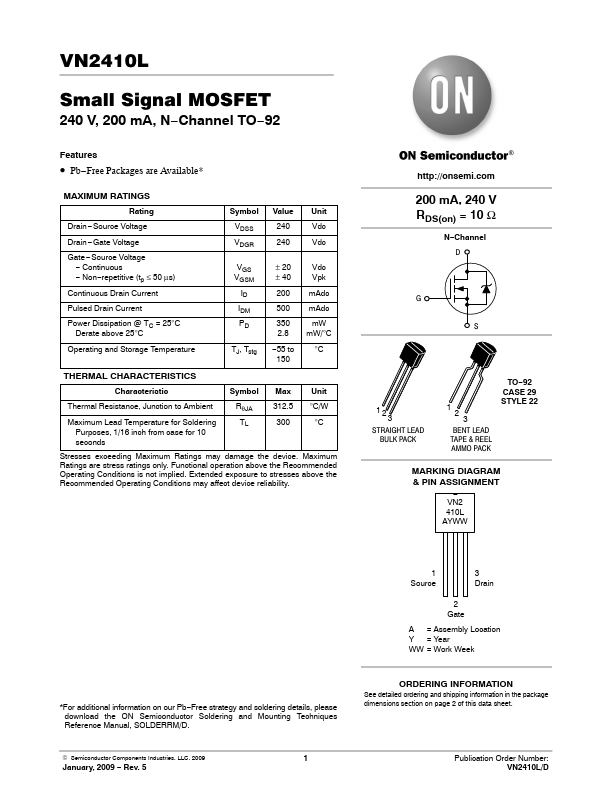
The following content is an automatically extracted verbatim text
from the original manufacturer datasheet and is provided for reference purposes only.
View original datasheet text
VN2410L
Small Signal MOSFET
240 V, 200 mA, N−Channel TO−92
Features
• Pb−Free Packages are Available*
MAXIMUM RATINGS
Rating
Symbol Value Unit
Drain −Source Voltage
Drain −Gate Voltage
Gate −Source Voltage − Continuous − Non−repetitive (tp ≤ 50 μs)
Continuous Drain Current
Pulsed Drain Current
Power Dissipation @ TC = 25°C Derate above 25°C
VDSS VDGR
VGS VGSM
ID IDM PD
240
Vdc
240
Vdc
± 20
Vdc
± 40
Vpk
200 mAdc
500 mAdc
350
mW
2.8 mW/°C
Operating and Storage Temperature
TJ, Tstg −55 to
°C
150
THERMAL CHARACTERISTICS
Characteristic
Symbol Max Unit
Thermal Resistance, Junction to Ambient
RθJA
312.5 °C/W
Maximum Lead Temperature for Soldering
TL
Purposes, 1/16 inch from case for 10
seconds
300
°C
Stresses exceeding Maximum Ratings may damage the device.