25FU406C Description
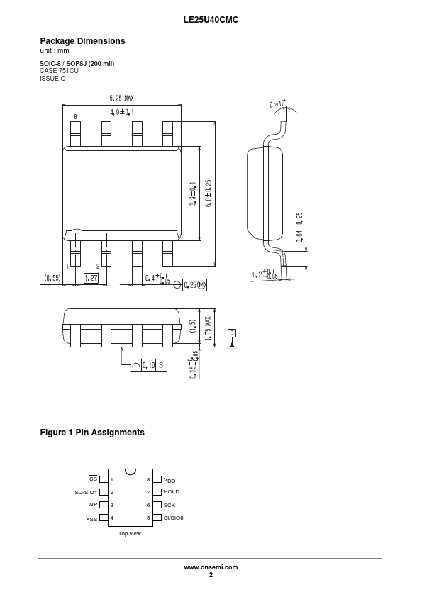
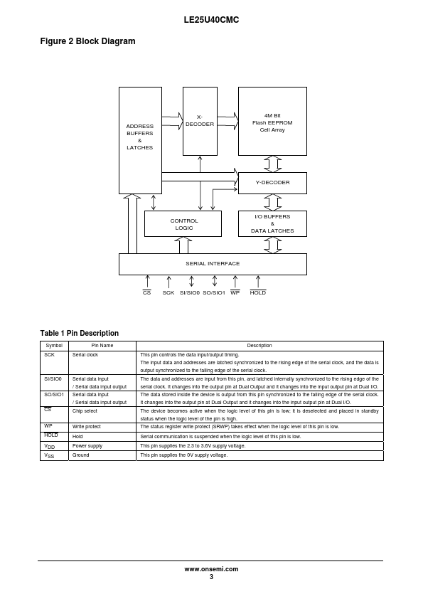
Symbol SCK Pin Name Serial clock SI/SIO0 SO/SIO1 CS Serial data input / Serial data input output Serial data input / Serial data input output Chip select WP HOLD VDD VSS Write protect Hold Power supply Ground Description This pin controls the data input/output timing. The input data and addresses are latched synchronized to the rising edge of the serial clock, and the data is output synchronized to the falling edge...
25FU406C Applications
- This product is licensed from Silicon Storage Technology, Inc. (USA)