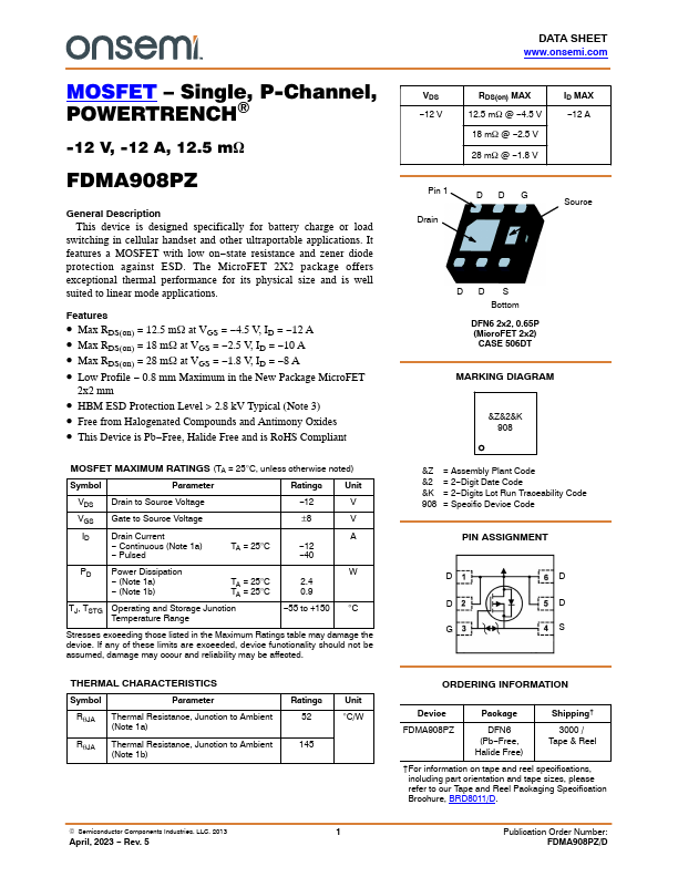
FDMA908PZ Overview
Description
This device is designed specifically for battery charge or load switching in cellular handset and other ultraportable applications. It features a MOSFET with low on-state resistance and zener diode protection against ESD.
Key Features
- Max RDS(on) = 12.5 mW at VGS = -4.5 V, ID = -12 A
- Max RDS(on) = 18 mW at VGS = -2.5 V, ID = -10 A
- Max RDS(on) = 28 mW at VGS = -1.8 V, ID = -8 A
- 0.8 mm Maximum in the New Package MicroFET 2x2 mm
- HBM ESD Protection Level > 2.8 kV Typical (Note
- Free from Halogenated Compounds and Antimony Oxides
- This Device is Pb-Free, Halide Free and is RoHS Compliant MOSFET Symbol Parameter Ratings Unit VDS Drain to Source Voltage
- 12 V VGS Gate to Source Voltage ±8 V ID Drain Current A
- Continuous (Note 1a) TA = 25°C
- 40 PD Power Dissipation