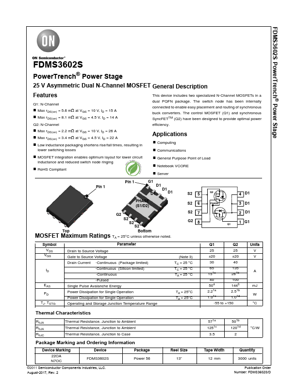
FDMS3602S Description
N-Channel Max rDS(on) = 5.6 mΩ at VGS = 10 V, ID = 15 A Max rDS(on) = 8.1 mΩ at VGS = 4.5 V, ID = 14 A Q2: N-Channel Max rDS(on) = 2.2 mΩ at VGS = 10 V, ID = 26 A Max rDS(on) = 3.4 mΩ at VGS = 4.5 V, ID = 22 A Low inductance packaging shortens rise/fall times, resulting in lower switching losses MOSFET integration enables optimum layout for lower circuit inductance and reduced switch node ringing RoHS...
FDMS3602S Key Features
- Max rDS(on) = 5.6 mΩ at VGS = 10 V, ID = 15 A
- Max rDS(on) = 8.1 mΩ at VGS = 4.5 V, ID = 14 A
- Max rDS(on) = 2.2 mΩ at VGS = 10 V, ID = 26 A
- Max rDS(on) = 3.4 mΩ at VGS = 4.5 V, ID = 22 A
- MOSFET integration enables optimum layout for lower circuit inductance and reduced switch node ringing
- RoHS pliant
FDMS3602S Applications
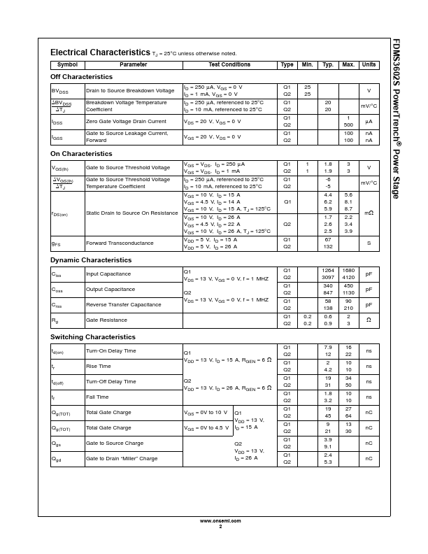
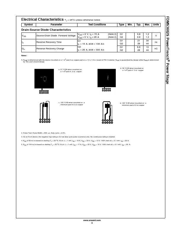
- Continuous (Silicon limited) -Continuous -Pulsed Single Pulse Avalanche Energy Power Dissipation for Single Operation Power Dissipation for Single Operation Ope