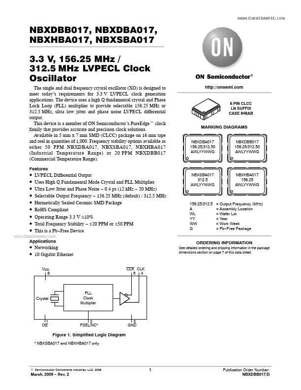
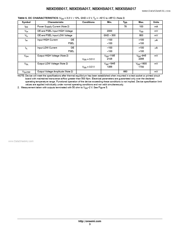
NBXDBB017 Description
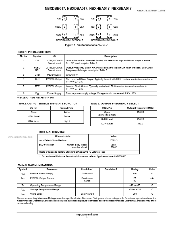
LVTTL/LVCMOS Control Input LVTTL/LVCMOS Control Input Power Supply Output Enable Pin. When left floating pin defaults to logic HIGH and output is active. See OE pin description Table.
NBXDBB017 Key Features
- LVPECL Differential Output Uses High Q Fundamental Mode Crystal and PLL Multiplier Ultra Low Jitter and Phase Noise
- 0.4 ps (12 kHz
- 20 MHz) Selectable Output Frequency
- 156.25 MHz (default) / 312.5 MHz Hermetically Sealed Ceramic SMD Package RoHS pliant Operating Range 3.3 V ±10% Total Fr
- ±20 PPM or ±50 PPM This is a Pb-Free Device